Difference between revisions of "Orchard Electronics Developer's Guide"
(→MCU) |
(→Schematics) |
||
| Line 20: | Line 20: | ||
We steered clear of using any of the DIO pins for any GPIO purposes. We opted to connect the RF packet ready and transmission FIFO not full (TX_CAN) pins, so that we could use interrupts to drive automatic FIFO filling and draining for reliable implementation of larger packet lengths without busy-waiting the CPU in a thread monitoring FIFO status. | We steered clear of using any of the DIO pins for any GPIO purposes. We opted to connect the RF packet ready and transmission FIFO not full (TX_CAN) pins, so that we could use interrupts to drive automatic FIFO filling and draining for reliable implementation of larger packet lengths without busy-waiting the CPU in a thread monitoring FIFO status. | ||
| − | |||
| − | |||
'''GPIO Expander''' | '''GPIO Expander''' | ||
| Line 29: | Line 27: | ||
'''LDO''' | '''LDO''' | ||
| − | The LP3982 LDO is a reasonably inexpensive LDO (~$0.20) with very low dropout, good noise performance, and 90uA quiescent current. Cheaper LDOs can be substituted, but compared to the cost of other components in the system it seemed like a reasonable compromise between cost and performance. | + | The LP3982 LDO is a reasonably inexpensive LDO (~$0.20) with very low dropout, good noise performance, and 90uA quiescent current. Cheaper LDOs can be substituted, but compared to the cost of other components in the system it seemed like a reasonable compromise between cost and performance. Also, I generally find that Nat Semi/TI regulators have better short circuit protection than the Chinese clones, and this is a desirable property for a dev platform. |
| + | |||
| + | The quiescent current is a bit high compared to the ultimate performance achievable by the Kinetis-W (330nA in VLLS0), but reasonable compared to Stop mode (212uA). A number of other peripherals consume current on the order of dozens of uA in standby. This metric could be improved if you're looking for extremely long battery life with the system in low power stop mode most of the time. | ||
| − | The | + | The LDO is slaved directly off the battery, not the boost regulator, for better efficiency. The low dropout allows for operation even when the battery is quite low. |
The 300mA output of the LDO is ample for the system. | The 300mA output of the LDO is ample for the system. | ||
| + | |||
| + | '''SWD''' | ||
| + | The SWD pins are multiplexed with some of the touch sensor pads on the Kinetis W, which is yet another reason we opted to use an external captouch chip. The Kinetis W relies entirely upon SWD for provisioning the chip's flash memory, and thus any captouch pad design has to anticipate the need for both SWD and electrode design. We didn't like this restriction. | ||
| + | |||
| + | We add a MCU reset pad as well for SWD. It's not necessary, but it could be handy. | ||
| + | |||
| + | As an interesting side note, the Kinetis W is so "bare metal" it has no internal mask ROM firmware as far as we can tell. A factory-new device will constantly stab itself in the eye on a fault condition as it tries to execute invalid code at the reset vector. SWD is thus essential to the factory provisioning system. | ||
| + | |||
| + | '''USB''' | ||
| + | For the purposes of charger type detection, we wire USB pins to analog inputs on the Kinetis-W. However, we also provided unpopulated board-level resistors to allow the opportunity for the Kinetis-W to respond as a low-speed USB device via bitbang protocol. The firmware isn't there to support it, but if someone writes that module the appropriate resistors are all there to allow for the device to work as a low-speed USB peripheral. | ||
| + | |||
| + | '''Other''' | ||
| + | We provide an FTDI 3.3V compatible header for serial console support. Nominal baud rate is 115200 8-N-1. Some variants of the design include a diode on the power pin so you could in theory power the board from the FTDI cable for debugging. However, once we realized that SWD was more useful than UART, we eliminated that diode in later variants. The diode is provided because we want to avoid back-powering the USB subsystem if the board is energized from other means. | ||
| + | |||
| + | The reset switch is just a simple push button with an RC to help filter out mechanical chatter. | ||
| + | |||
| + | The page also documents all the allocated I2C addresses and SPI allocations. We encourage designers who change the design to keep this table up to date, as it's quite helpful for firmware engineers. | ||
| + | |||
| + | As an administrative note, we use the schematic symbols "NT" to indicate components that are part of the BOM but not assembled onto the board. So, for example, the firmware and the antenna (which screws into the SMA edge launch socket) are NT symbols. | ||
===Charger & Battery=== | ===Charger & Battery=== | ||
| + | There's a few architectural options. The two basic directions enabled are: | ||
| + | |||
| + | * Big, brawny, and expensive | ||
| + | * Small and cheap | ||
| + | |||
http://bunniefoo.com/orchard/hardware/orchard-charger.png | http://bunniefoo.com/orchard/hardware/orchard-charger.png | ||
| + | |||
| + | '''Big and Brawny''' | ||
| + | For designs that need beefy batteries (>1500mAh), a BQ24260 charger is invoked. It's not cheap, but this charger can fully utilizes the current available on a CDP (at 1.5A) to charge larger batteries. It also has an integral boost regulator, so VUSB (the +5V line) can be powered up even if a charger is not present. This boost regulator is essential for driving features such as the WS2812B LED which requires a +5V source, and thus it's a nice 2-in-1 solution. | ||
| + | |||
| + | We never validated the battery temperature sensor feature on the BQ24260, as none of our batteries have an integral temperature sensor. But, the calculations are based upon a 103-AT style thermistor with a beta of 3435 kelvin and a nominal resistance of 10k at 25 degrees C. | ||
| + | |||
| + | The inductor calculations for the BQ24260 are also documented on the page. I have a preference for coilcraft inductors, and the LPS4018 is a nice low profile solution with high saturation current for its size. | ||
| + | |||
| + | I opted to use multiple parallel filter caps on VBAT_SYS instead of a single larger one to reduce ESR and also simplify the BOM. Since this design is intended for smaller runs, quadrupling-down on 10uF capacitors means you burn through a reel of the parts faster. Using a 47uF cap would be both more expensive and also more parts wasted at the end of a short run. However, if board space is a premium, then condensing C16B-C19B into a single part is warranted. | ||
| + | |||
| + | We felt that the internal conduction loss of the system transistor for the BQ24260 is adequate, and thus we don't use an external transistor via BGATE. | ||
| + | |||
| + | BQ24260 is a variant of the regulator that features automatic D+/D- recognition. In practice, we found that the feature works so-so, especially if you're relying upon the system to boost voltage; for unknown reasons the charger capacity identification would tend to fail. Instead, we mapped microcontroller pins to D+/D- and do charger detection that way and override the BQ24260's readings. | ||
| + | |||
| + | One neat feature of the BQ24260 is it also supports auto charge rate reduction if the input voltage is seen to be drooping. | ||
| + | |||
| + | All of these features come at a small burden on the firmware, i.e., the chip needs a bit of configuration, and it also requires to be constantly pinged by a watchdog while in boost or in charging mode. The requisite firmware to do this is fairly complete. | ||
| + | |||
| + | http://bunniefoo.com/orchard/hardware/orchard-battery-alt.png | ||
| + | |||
| + | '''Small and cheap''' | ||
| + | On some variants of the design, pads are provided to alternately populate an MCP73812T. Note that we never validated this circuit, but it's there in case someone wants to try it. This is a cheap, single-chip linear regulator charging solution set to 500mA with a resistor. According to the datasheet, it pretty much just "does the right thing" without any firmware programming. | ||
| + | |||
| + | '''Gas Gauge options''' | ||
| + | We provide two gas gauge options: impedance tracking, and voltage tracking. | ||
===Sensors=== | ===Sensors=== | ||
Revision as of 18:59, 5 June 2015
Contents
Design Guide
Schematics
A page-by-page discussion of the Orchard schematics.
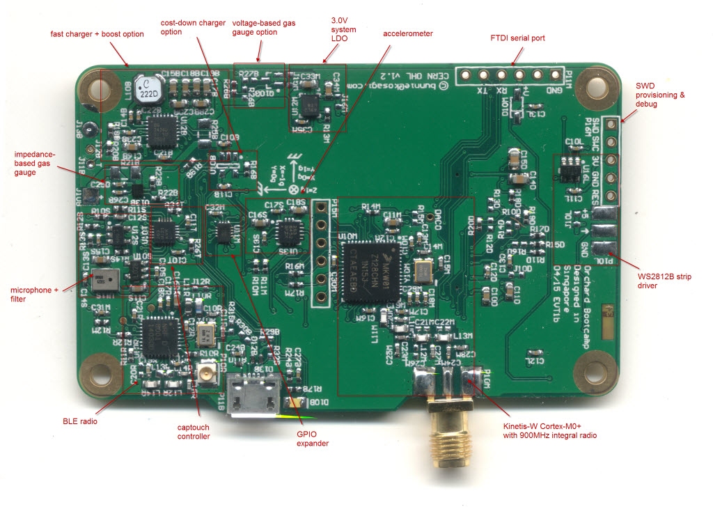
MCU
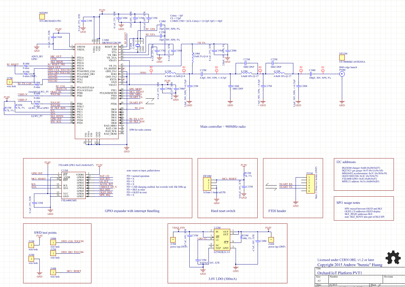
This page contains the Kinetis-W MCU, RF filter, GPIO expander, system LDO, reset switch and various test points.
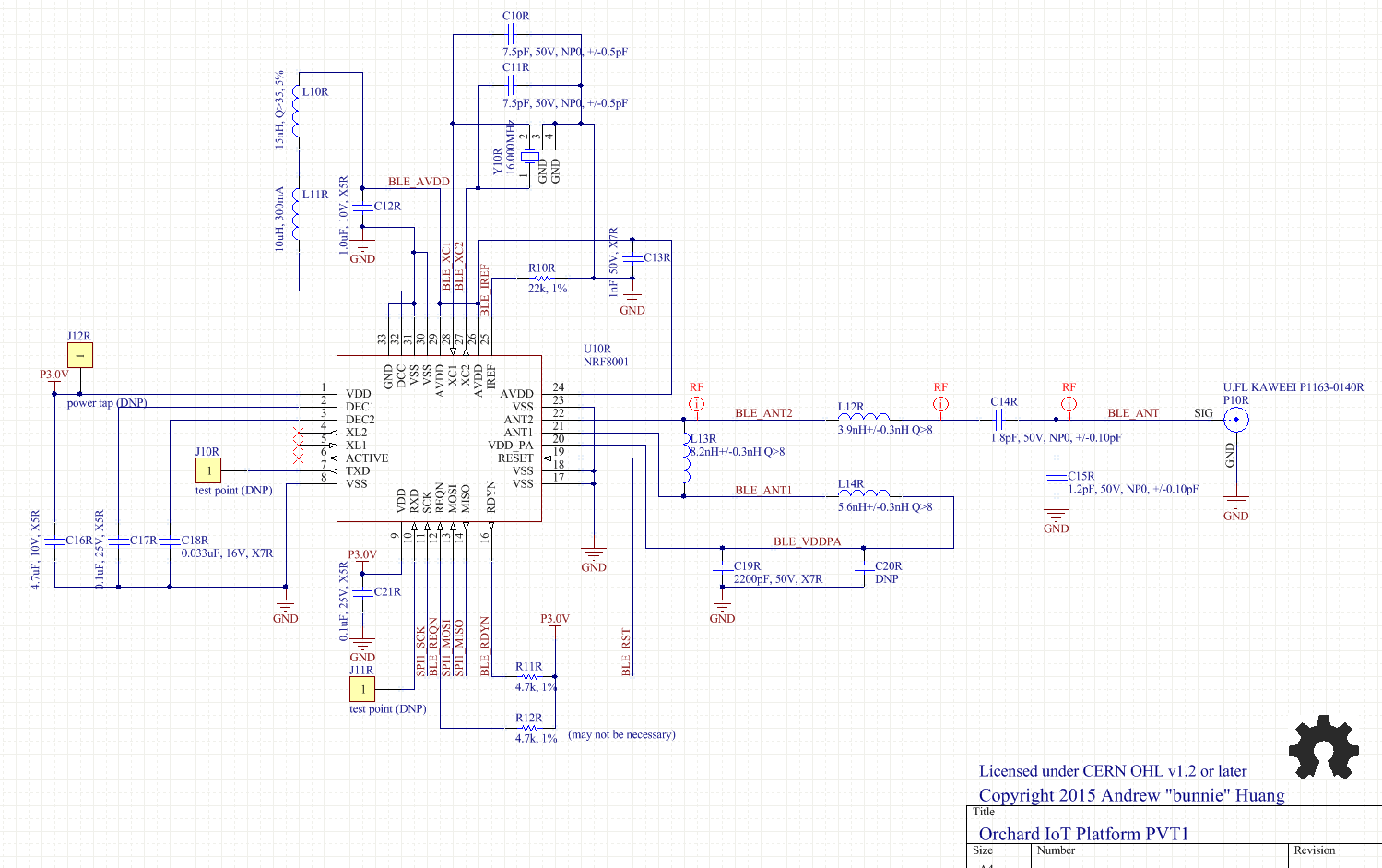
CPU Design Notes The RF filter topology and component values are directly from the Freescale reference design for 900-MHz band radios. The component selection has been fine-tuned a bit to support low-cost China vendors without too much loss in performance. In lab testing, the series inductors L12M and L13M seem to be the greatest contributor to insertion loss, and thus those were upgraded to wirewound inductors from MLC inductors. We are using an SMA edge-launch connector for the antenna, but the design could also be adapted to use a microstrip, on-board cermaic, or U.FL connector depending upon the user's needs.
The accuracy of the crystal on the Kinetis-W is greatly affected by the load capacitance. On our initial prototype, we had a crystal with a CL of around 7pF, and then we switched to one with a 12pF CL without changing the parallel capacitors. That offset caused enough frequency shift to cause high bit error rates in data demodulation. So pay attention to the ppm tolerance of the crystal as well as the CL if you are re-designing that circuit.
We moved RF_RESET from its default location of PTE30 on the reference design to PTE19. The reason is that PTE30 is the one and only DAC output, and it seemed like a shame to waste it on a reset line for the radio.
Another trap on the design is that port B on the microcontroller is the only port that cannot be used to trigger interrupts. Thus, when wiring up interrupt sources to the MCU, avoid port B.
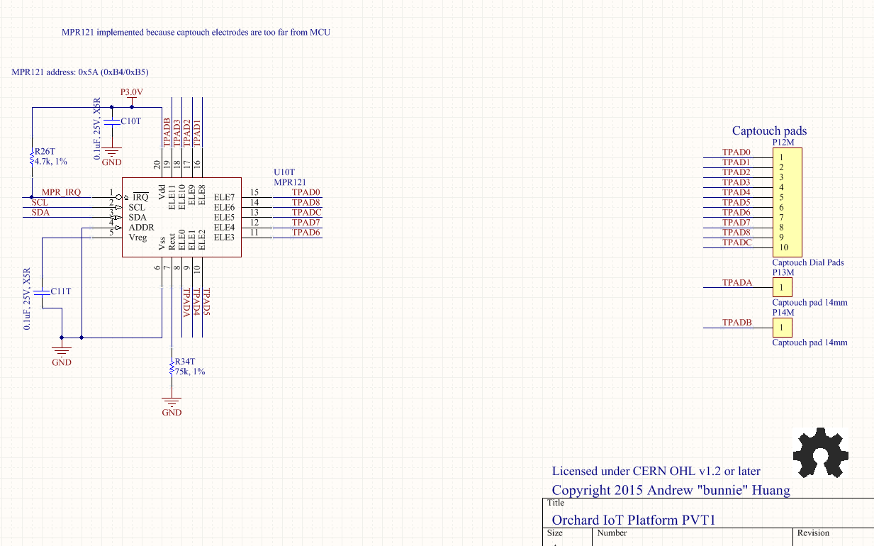
While the Kinetis MCU supports captouch on its own, we opted not to use the facility because it's poorly documented, and the scant documentation we could find indicated that the traces should be shorter than about 4-5". The problem is that we wanted to co-locate the MCU next to the RF port, which isn't always convenient for captouch surfaces. Thus to improve our chances of first-time success, we opted to use an external captouch chip with better documentation and board location.
We steered clear of using any of the DIO pins for any GPIO purposes. We opted to connect the RF packet ready and transmission FIFO not full (TX_CAN) pins, so that we could use interrupts to drive automatic FIFO filling and draining for reliable implementation of larger packet lengths without busy-waiting the CPU in a thread monitoring FIFO status.
GPIO Expander Although we could just barely cram all the signals into the MCU for the base design, as a platform we needed to have some free pins for extensibility. Thus, we included a GPIO expander. For cost-down designs that don't need to support such a rich set of peripherals, one could certainly cut the GPIO expander from the design and rework the firmware to use direct GPIO mappings.
Our choice of which pins to route to the GPIO expander was primarily static signals (reset lines, charger status lines) and less time sensitive interrupts. The GPIO expander can aggregate interrupts and fire a single pin that's then handled by firmware that queries the exact interrupt source and dispatches the correct routine based on that query.
LDO The LP3982 LDO is a reasonably inexpensive LDO (~$0.20) with very low dropout, good noise performance, and 90uA quiescent current. Cheaper LDOs can be substituted, but compared to the cost of other components in the system it seemed like a reasonable compromise between cost and performance. Also, I generally find that Nat Semi/TI regulators have better short circuit protection than the Chinese clones, and this is a desirable property for a dev platform.
The quiescent current is a bit high compared to the ultimate performance achievable by the Kinetis-W (330nA in VLLS0), but reasonable compared to Stop mode (212uA). A number of other peripherals consume current on the order of dozens of uA in standby. This metric could be improved if you're looking for extremely long battery life with the system in low power stop mode most of the time.
The LDO is slaved directly off the battery, not the boost regulator, for better efficiency. The low dropout allows for operation even when the battery is quite low.
The 300mA output of the LDO is ample for the system.
SWD The SWD pins are multiplexed with some of the touch sensor pads on the Kinetis W, which is yet another reason we opted to use an external captouch chip. The Kinetis W relies entirely upon SWD for provisioning the chip's flash memory, and thus any captouch pad design has to anticipate the need for both SWD and electrode design. We didn't like this restriction.
We add a MCU reset pad as well for SWD. It's not necessary, but it could be handy.
As an interesting side note, the Kinetis W is so "bare metal" it has no internal mask ROM firmware as far as we can tell. A factory-new device will constantly stab itself in the eye on a fault condition as it tries to execute invalid code at the reset vector. SWD is thus essential to the factory provisioning system.
USB For the purposes of charger type detection, we wire USB pins to analog inputs on the Kinetis-W. However, we also provided unpopulated board-level resistors to allow the opportunity for the Kinetis-W to respond as a low-speed USB device via bitbang protocol. The firmware isn't there to support it, but if someone writes that module the appropriate resistors are all there to allow for the device to work as a low-speed USB peripheral.
Other We provide an FTDI 3.3V compatible header for serial console support. Nominal baud rate is 115200 8-N-1. Some variants of the design include a diode on the power pin so you could in theory power the board from the FTDI cable for debugging. However, once we realized that SWD was more useful than UART, we eliminated that diode in later variants. The diode is provided because we want to avoid back-powering the USB subsystem if the board is energized from other means.
The reset switch is just a simple push button with an RC to help filter out mechanical chatter.
The page also documents all the allocated I2C addresses and SPI allocations. We encourage designers who change the design to keep this table up to date, as it's quite helpful for firmware engineers.
As an administrative note, we use the schematic symbols "NT" to indicate components that are part of the BOM but not assembled onto the board. So, for example, the firmware and the antenna (which screws into the SMA edge launch socket) are NT symbols.
Charger & Battery
There's a few architectural options. The two basic directions enabled are:
- Big, brawny, and expensive
- Small and cheap
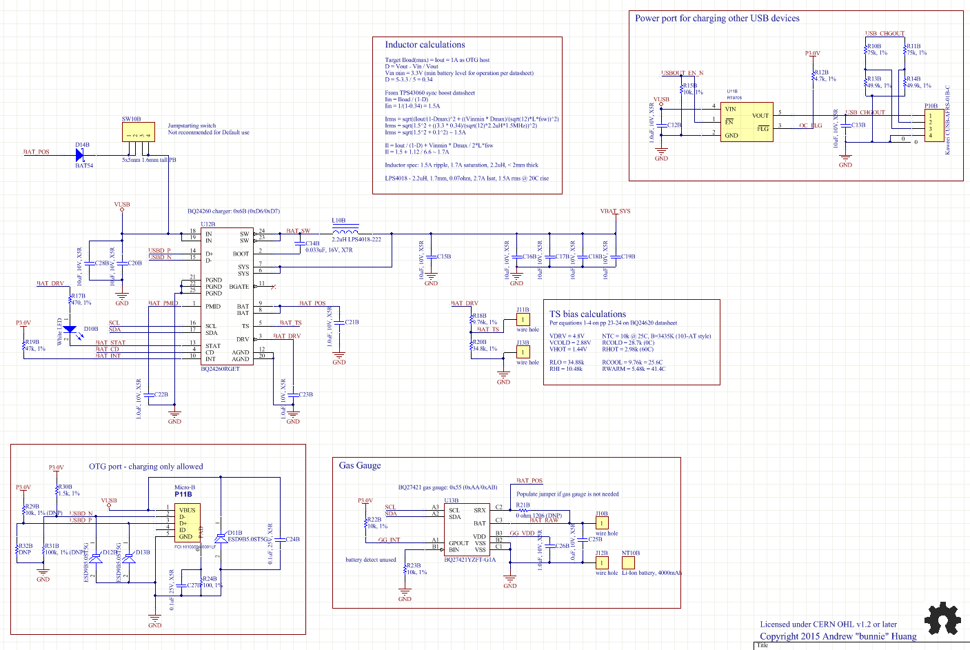
Big and Brawny For designs that need beefy batteries (>1500mAh), a BQ24260 charger is invoked. It's not cheap, but this charger can fully utilizes the current available on a CDP (at 1.5A) to charge larger batteries. It also has an integral boost regulator, so VUSB (the +5V line) can be powered up even if a charger is not present. This boost regulator is essential for driving features such as the WS2812B LED which requires a +5V source, and thus it's a nice 2-in-1 solution.
We never validated the battery temperature sensor feature on the BQ24260, as none of our batteries have an integral temperature sensor. But, the calculations are based upon a 103-AT style thermistor with a beta of 3435 kelvin and a nominal resistance of 10k at 25 degrees C.
The inductor calculations for the BQ24260 are also documented on the page. I have a preference for coilcraft inductors, and the LPS4018 is a nice low profile solution with high saturation current for its size.
I opted to use multiple parallel filter caps on VBAT_SYS instead of a single larger one to reduce ESR and also simplify the BOM. Since this design is intended for smaller runs, quadrupling-down on 10uF capacitors means you burn through a reel of the parts faster. Using a 47uF cap would be both more expensive and also more parts wasted at the end of a short run. However, if board space is a premium, then condensing C16B-C19B into a single part is warranted.
We felt that the internal conduction loss of the system transistor for the BQ24260 is adequate, and thus we don't use an external transistor via BGATE.
BQ24260 is a variant of the regulator that features automatic D+/D- recognition. In practice, we found that the feature works so-so, especially if you're relying upon the system to boost voltage; for unknown reasons the charger capacity identification would tend to fail. Instead, we mapped microcontroller pins to D+/D- and do charger detection that way and override the BQ24260's readings.
One neat feature of the BQ24260 is it also supports auto charge rate reduction if the input voltage is seen to be drooping.
All of these features come at a small burden on the firmware, i.e., the chip needs a bit of configuration, and it also requires to be constantly pinged by a watchdog while in boost or in charging mode. The requisite firmware to do this is fairly complete.
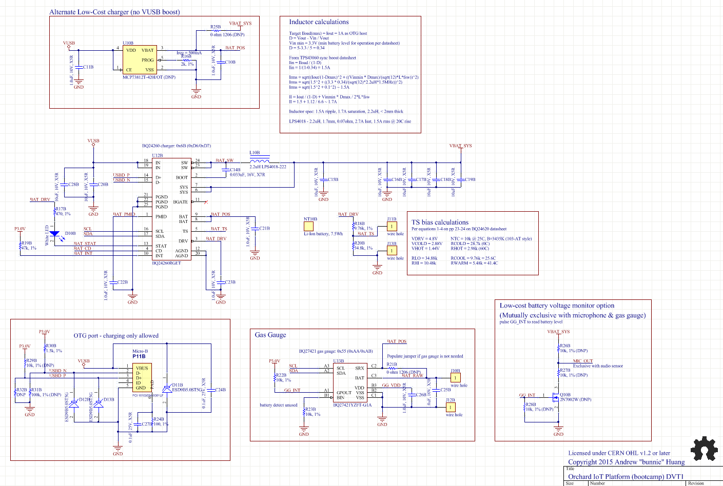
Small and cheap On some variants of the design, pads are provided to alternately populate an MCP73812T. Note that we never validated this circuit, but it's there in case someone wants to try it. This is a cheap, single-chip linear regulator charging solution set to 500mA with a resistor. According to the datasheet, it pretty much just "does the right thing" without any firmware programming.
Gas Gauge options We provide two gas gauge options: impedance tracking, and voltage tracking.
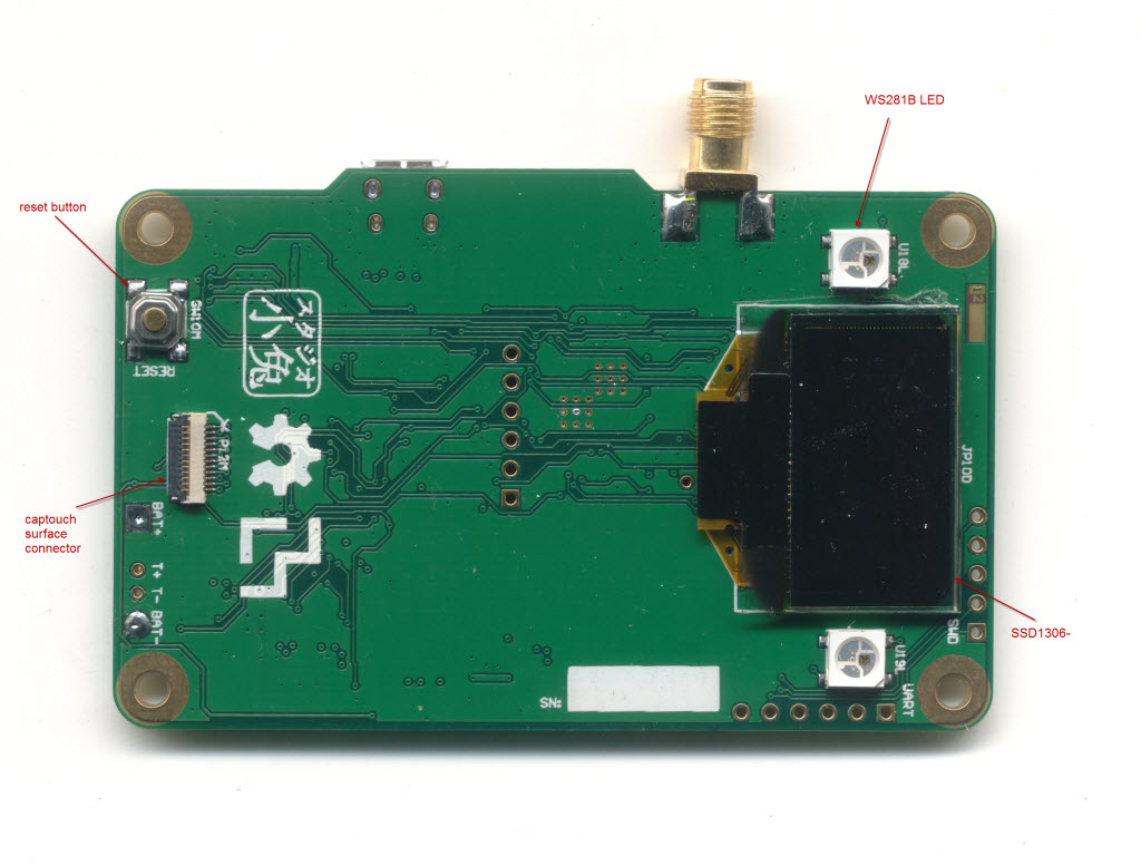
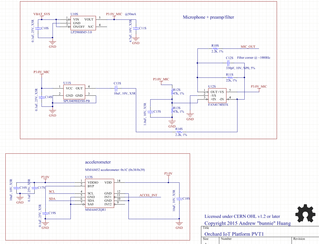
Sensors
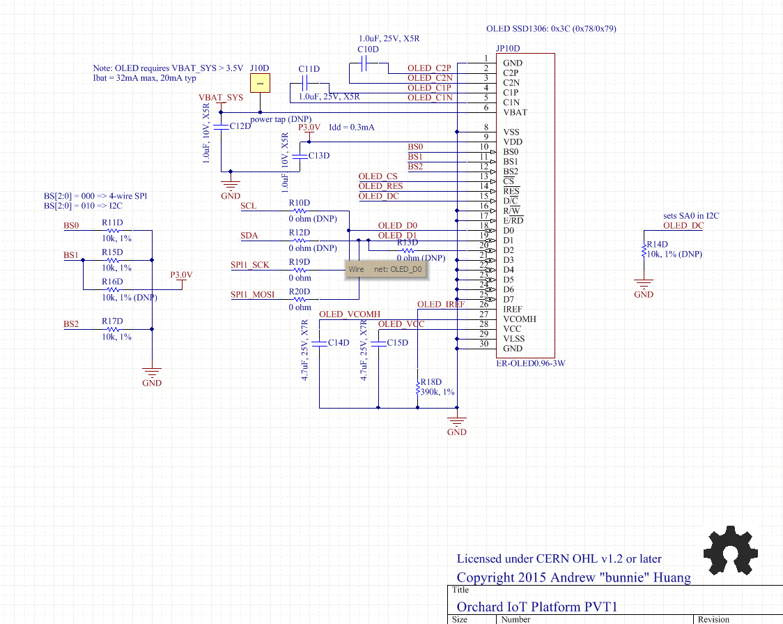
OLED
BLE
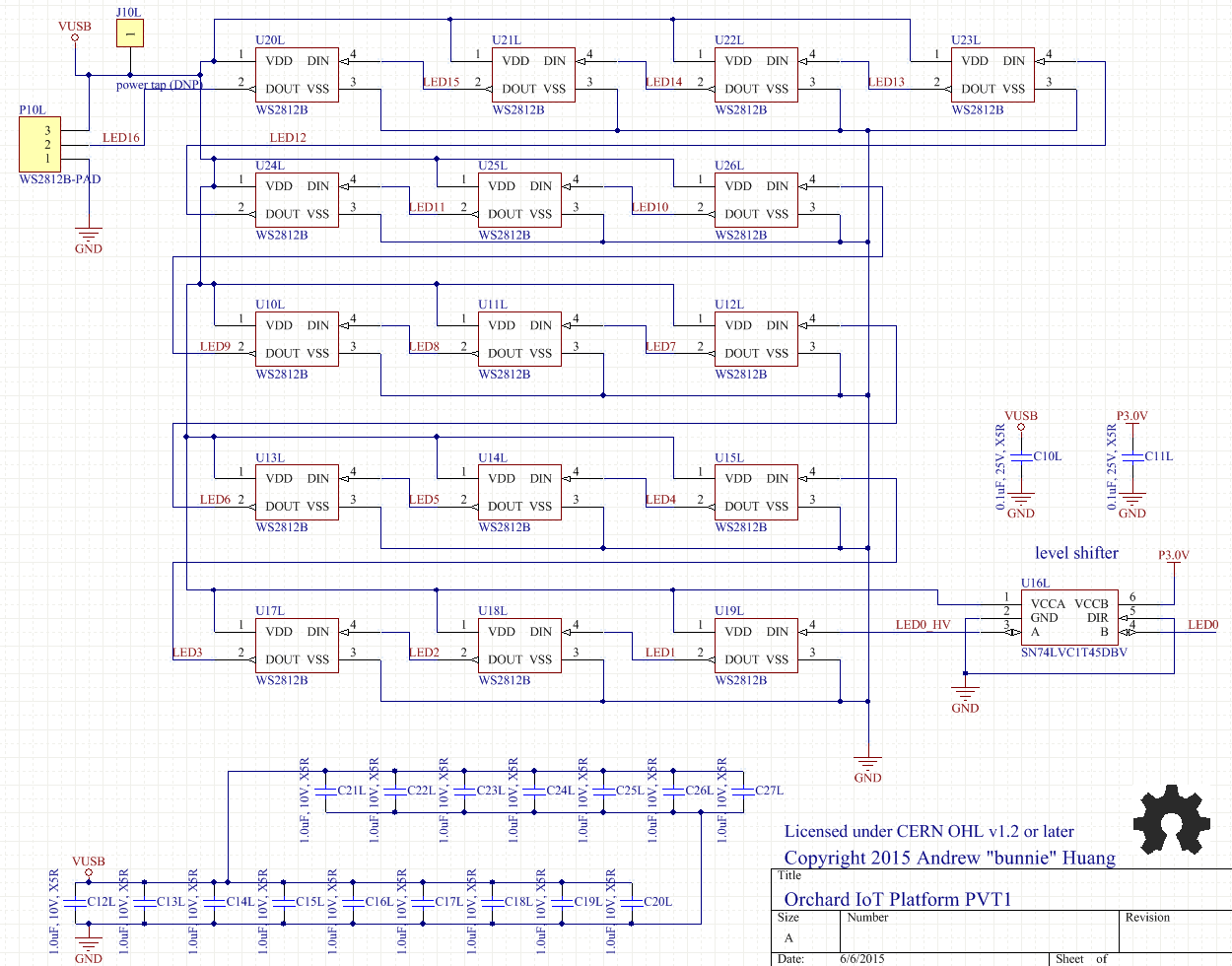
LED
Captouch
High-Res Photo Guide