GPBB User Guide
The GPBB is a good entry point for most hardware hacking applications on Novena. This document describes in some detail about the function and theory of operation behind the GPBB.
Contents
GPBB Features
- Digital I/O
- 16 digital outputs organized in two 8-bit banks (A and B)
- Each bank can be individually tri-stated
- 8 digital inputs organized in a single 8-bit bank
- Switchable I/O voltage
- I/O VDD software switchable between +5V and a lower voltage
- Lower voltage I/O VDD nominally set to 3.3V but adjustable changing out a single resistor
- I/O VDD current-limited to 500mA
- In 5V mode, overcurrent indicator available
- I/O VDD can be sampled by on-board ADC to verify operation
- LEDs
- Four green LEDs
- Connected to port B bits 0-3
- Analog Input
- 6x 10-bit analog inputs
- 0-4.7V full scale range
- AVDD set by local LDO to +/- 1.5% accuracy
- Up to 200 ksps conversion rate
- Upgradable to 12-bit accuracy by swapping out ADC chip
- DAC-to-ADC loopback and VDD/IO measurement paths available
- Analog output
- 2x 10-bit analog outputs
- 0-3.3V full scale range
- Output speed limited by I2C bus rate (100kHz I2C -> ~5kHz output rate)
- Upgradable to 12-bit accuracy by swapping out DAC chips
GPBB Host Interface Features
The host interface to the GPBB is implemented using the FPGA. It is configurable, and therefore, this feature list should not be considered etched in stone. There is a lot of flexibility on how to implement the host interface, and this particular configuration was chosen to maximize the pedagogical value of the GPBB reference design.
- EIM register interface
- Modular, scalable register interface
- FPGA version reporting
- Loopback testing
- Control of the digital input and output ports
- CPU-> FPGA I2C register interface
- Example of communicating with the FPGA via I2C
- Control and readout of the ADC
- FPGA version reporting
- Loopback testing
- CPU->DAC I2C interface
- Direct bus interface to I2C with expansion card components
- Example of using expansion port with no FPGA intervention
- 2x DAC chips connected to CPU I2C bus
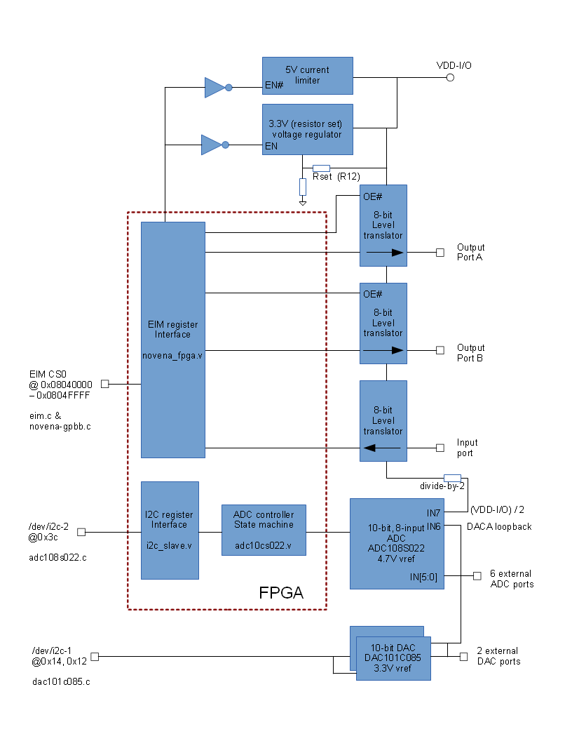
Block Diagram

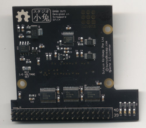
Hardware Photo

Note R12, the voltage set resistor, is in the mid-left of the board in this photo.
Setting the I/O Voltage
The low voltage setting for the I/O is defaulted to 3.3V.
You can change this by desoldering R12, the larger 1206 resistor, and replacing it with one of the following:
- 316 ohm for 3.3V (default)
- 215 ohm for 2.5V
- 124 ohm for 1.8V
If you don't want to desolder the 316 ohm resistor, you can:
- Parallel a 680 ohm resistor with the default 316 ohm resistor to get 215 ohms
- Parallel a 200 ohm resistor with the default 316 ohm resistor to get 122 ohms
The 1206 resistor is large enough so one can fairly easily parallel an axial resistor across the surface-mount device.
Command-line Firmware Example
A command-line example program of using the GPBB can be found on github at
https://github.com/bunnie/novena-gpbb-example
Before running the example program, you must configure the FPGA. You can do so using the shell script included in the above git repo as follows:
sudo ./configure.sh novena_fpga.bit
The shell script basically configures the FPGA configuration reset pin, flips it (so the FPGA is erased), and then dd's the bitfile to /dev/spidev2.0.
The example program must be run as sudo, as it uses the /dev/mem interface to access the memory-mapped EIM CS0 and CS1 regions.
The built-in help describes the usage of the program:
bunnie@bunnie-novena-laptop:~/code/novena-gpbb-example$ sudo ./novena-gpbb
Usage:
./novena-gpbb [-h]
        -h  This help message
        -v  Read out the version code of the FPGA
        -da <value> set DAC A to value (0-1024 decimal)
        -db <value> set DAC B to value (0-1024 decimal)
        -a  <chan> set and read channel <chan> from ADC
        -hv set VDD-IO to high (5V) voltage
        -lv set VDD-IO to low (nom 3.3V unless you trimmed it) voltage
        * GPBB has two 8-bit output-only ports (A,B), and one 8-bit input port
        -oea <value> drive I/O bank A (value = 1 means drive, 0 means tristate)
        -oeb <value> drive I/O bank B (value = 1 means drive, 0 means tristate)
        -p <port> return last written <port> value in hex, port is [a,b] (note these ports are output-only)
        -p <port> <hex value> set <port> to <hex value>
        -p_set <port> <bit>  set <port> <bit>
        -p_clr <port> <bit>  clear <port> <bit>
        -rp return the value of the 8-bit input port
        * CS1 isn't useful in the design, but loopback code provided as a template
        -testcs1 Check that burst-access area (CS1) works
The test program incorporates all three interfaces (EIM CS0, I2C-1, and I2C-2) to drive the various interfaces. It also has an EIM CS1 example to mirror the example of using the burst-mode CS1 interface.
Burst-mode EIM access is provided for applications that require a high bus utilization. The i.MX6 takes about 32 cycles to turn the bus around between burst memory operations to the region. Thus, the CS0 interface, which transfers only one 16-bit word at a time, can achieve only about 3% utilization of the bus. Burst mode will perform a 64-bit access (4 words in an access) trivially, and can extend to much longer bursts with properly coded FPGA hardware. Even using the 64-bit accesses triples utilization to 10%. The example implemented in this codebase just does a loopback write/read of the CS1 space.
FPGA Details
The FPGA implementation can be found at
https://github.com/bunnie/novena-gpbb-fpga
The design is targeted to a Xilinx Webpack ISE "PlanAhead" flow (downloadable for free (but not open source) to run on x86 machines), so the novena-gpbb.ppr file would be the project container. This code is tested against Webpack ISE version 14.5 and can achieve 100% timing closure.
Project Structure
For those who have never used a Xilinx FPGA project before, there are a few things to be aware of.
- There is a constraints file (I refer to it as a ".UCF"), novena.ucf, that maps logical top-level ports to physical pins, and also sets timing parameters to guide the place & route engine.
- Xilinx features "IP" blocks that are defined using XML (such as bclk_dll.xci and synthesized using their CORE Generator tool. This design features three IP blocks, all of them for clock and timing management.
- The directory structure of the github repo matches the default structure that the Xilinx PlanAhead tool generates.
- There is a top-level PlanAhead project descriptor file called novena-gpbb.ppr.
Code Architecture
There is a top-level file, novena_fpga.v, which contains the following:
- FPGA logical I/O definition (in the module header)
- Instantiation of the ADC state machine
- EIM register set implementation
- I2C module
- Master reset synchronizer
- Three DLLs for clock skew management
- Manually instantiated I/O primitives
- The "heartbeat" LED counter
Pin mapping convention and UCF tour
By convention I use the PCB schematic names as much as possible for the FPGA top-level logical I/O definition, so you don't need to go into the .UCF to figure out what PCB trace goes to what inside. Then, I use a set of assign statements to map the physical I/Os to internal meanings. So, for example, you'll see
output wire F_LVDS_P11,
output wire F_LVDS_N11,
output wire F_DX,
etc. If you look at the schematic, you'll see these are names used on the expansion header that corresponds to very specific pin mappings. These are mapped to a "meaning" later on using
  assign F_LVDS_P11 = cpu_to_dutB[0];   // LED 0
  assign F_LVDS_N11 = cpu_to_dutB[1];   // LED 1
  assign F_DX1 = cpu_to_dutB[2];        // LED 2
The FPGA top-level logical I/O definitions are mapped to physical FPGA pins in the .UCF file, e.g.:
NET "F_LVDS_N11" LOC = T11;
NET "F_LVDS_N11" IOSTANDARD = LVCMOS33;
NET "F_LVDS_N11" SLEW = SLOW;
NET "F_LVDS_P11" LOC = R11;
NET "F_LVDS_P11" IOSTANDARD = LVCMOS33;
NET "F_LVDS_P11" SLEW = SLOW;
As you can see, in the .UCF logical names (F_LVDS_N11) get mapped to a package pin (T11), a well as assigned attributes such as the logic standard (LVCMOS33) and electrical properties (SLEW = SLOW). Other things like pull-ups, termination resistors and so forth can be added at this point. The most difficult bugs are often attributable to errors in the .UCF file, so don't forget that this file exists. To be clear, here are some headaches that happen with a wrong .UCF:
- Top-level FPGA logical pins that aren't in the .UCF (e.g. due to a typo) will be mapped by default to a random pin on the FPGA. This is no good.
- The slew rate spec of a pin can have a big impact on timing closure. However, you don't want to make all pins fast because there is a limit on how many fast-slew pins you can have that switch simultaneously (it's surprisingly low, search for SSO in this document for details on why).
.UCF also contains timing closure annotations, and placement directives, such as:
OFFSET = IN 4125 ps VALID 4750 ps BEFORE "bclk";
OFFSET = OUT 5100 ps AFTER "bclk";
The above sets the setup/hold time requirement for the EIM bus
NET "reg_wo_40010/state[*]" TIG;
NET "reg_wo_41012/state[*]" TIG;
The above tells the timing-driven place and route engine to ignore these register bits during timing closure, as they are driving asynchronous destinations. Relaxing which paths the place and route engine have to pay attention to helps your design compile faster and achieve better results on the paths that do matter.
INST "oddr2_eim0" IOB =FORCE;
INST "oddr2_eim1" IOB =FORCE;
The above tells the mapper to force primitives named oddr2_eim0 and oddr2_eim1 into the IOB (actually, now that I think of it, the ODDR prims probably go to an IOB by default but I introduced this constraint to make sure it's not optimized out by some other setting).
NET "bclk" TNM_NET = "bclk_tnm";
TIMESPEC TS_bclk = PERIOD "bclk_tnm" 133 MHz;
The above defines a "timing net" and assigns a clock period timespec to it, which tells the timing-driven place and route engine what speed it needs to achieve on your design to run at the EIM speed, e.g., 133MHz. Without this, it will just do whatever and compute for you the speed it achieved, which is often times lower than what you require for correct operation.