Difference between revisions of "Orchard Electronics Developer's Guide"
(→Design Guide) |
(→MCU) |
||
| Line 5: | Line 5: | ||
===MCU=== | ===MCU=== | ||
http://bunniefoo.com/orchard/hardware/orchard-mcu.png | http://bunniefoo.com/orchard/hardware/orchard-mcu.png | ||
| + | |||
| + | This page contains the Kinetis-W MCU, RF filter, GPIO expander, system LDO, reset switch and various test points. | ||
| + | |||
| + | '''CPU Design Notes''' | ||
| + | The RF filter topology and component values are directly from the Freescale reference design for 900-MHz band radios. The component selection has been fine-tuned a bit to support low-cost China vendors without too much loss in performance. In lab testing, the series inductors L12M and L13M seem to be the greatest contributor to insertion loss, and thus those were upgraded to wirewound inductors from MLC inductors. We are using an SMA edge-launch connector for the antenna, but the design could also be adapted to use a microstrip, on-board cermaic, or U.FL connector depending upon the user's needs. | ||
| + | |||
| + | The accuracy of the crystal on the Kinetis-W is greatly affected by the load capacitance. On our initial prototype, we had a crystal with a CL of around 7pF, and then we switched to one with a 12pF CL without changing the parallel capacitors. That offset caused enough frequency shift to cause high bit error rates in data demodulation. So pay attention to the ppm tolerance of the crystal as well as the CL if you are re-designing that circuit. | ||
| + | |||
| + | We moved RF_RESET from its default location of PTE30 on the reference design to PTE19. The reason is that PTE30 is the one and only DAC output, and it seemed like a shame to waste it on a reset line for the radio. | ||
| + | |||
| + | Another trap on the design is that port B on the microcontroller is the only port that cannot be used to trigger interrupts. Thus, when wiring up interrupt sources to the MCU, avoid port B. | ||
| + | |||
| + | While the Kinetis MCU supports captouch on its own, we opted not to use the facility because it's poorly documented, and the scant documentation we could find indicated that the traces should be shorter than about 4-5". The problem is that we wanted to co-locate the MCU next to the RF port, which isn't always convenient for captouch surfaces. Thus to improve our chances of first-time success, we opted to use an external captouch chip with better documentation and board location. | ||
| + | |||
| + | We steered clear of using any of the DIO pins for any GPIO purposes. We opted to connect the RF packet ready and transmission FIFO not full (TX_CAN) pins, so that we could use interrupts to drive automatic FIFO filling and draining for reliable implementation of larger packet lengths without busy-waiting the CPU in a thread monitoring FIFO status. | ||
| + | |||
| + | As an administrative note, we use the schematic symbols "NT" to indicate components that are part of the BOM but not assembled onto the board. So, for example, the firmware and the antenna (which screws into the SMA edge launch socket) are NT symbols. | ||
| + | |||
| + | '''GPIO Expander''' | ||
| + | Although we could just barely cram all the signals into the MCU for the base design, as a platform we needed to have some free pins for extensibility. Thus, we included a GPIO expander. For cost-down designs that don't need to support such a rich set of peripherals, one could certainly cut the GPIO expander from the design and rework the firmware to use direct GPIO mappings. | ||
| + | |||
| + | Our choice of which pins to route to the GPIO expander was primarily static signals (reset lines, charger status lines) and less time sensitive interrupts. The GPIO expander can aggregate interrupts and fire a single pin that's then handled by firmware that queries the exact interrupt source and dispatches the correct routine based on that query. | ||
| + | |||
| + | '''LDO''' | ||
| + | The LP3982 LDO is a reasonably inexpensive LDO (~$0.20) with very low dropout, good noise performance, and 90uA quiescent current. Cheaper LDOs can be substituted, but compared to the cost of other components in the system it seemed like a reasonable compromise between cost and performance. | ||
| + | |||
| + | The quiescent current is a bit high compared to the ultimate performance achievable by the Kinetis-W ( | ||
| + | |||
| + | The 300mA output of the LDO is ample for the system. | ||
===Charger & Battery=== | ===Charger & Battery=== | ||
Revision as of 18:32, 5 June 2015
Contents
Design Guide
Schematics
A page-by-page discussion of the Orchard schematics.
MCU
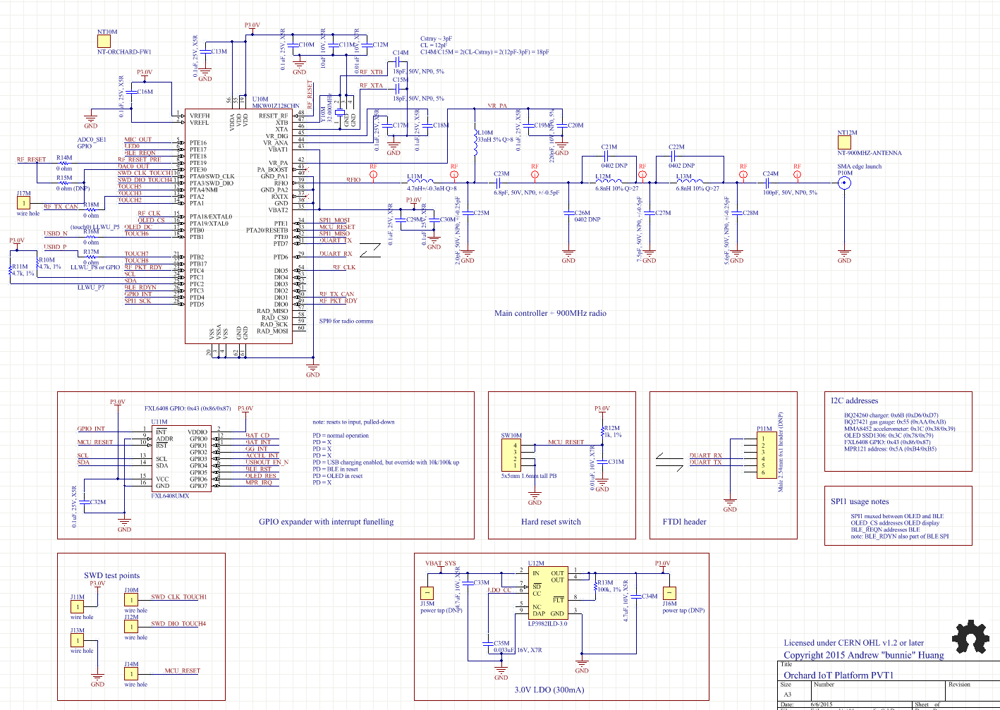
This page contains the Kinetis-W MCU, RF filter, GPIO expander, system LDO, reset switch and various test points.
CPU Design Notes The RF filter topology and component values are directly from the Freescale reference design for 900-MHz band radios. The component selection has been fine-tuned a bit to support low-cost China vendors without too much loss in performance. In lab testing, the series inductors L12M and L13M seem to be the greatest contributor to insertion loss, and thus those were upgraded to wirewound inductors from MLC inductors. We are using an SMA edge-launch connector for the antenna, but the design could also be adapted to use a microstrip, on-board cermaic, or U.FL connector depending upon the user's needs.
The accuracy of the crystal on the Kinetis-W is greatly affected by the load capacitance. On our initial prototype, we had a crystal with a CL of around 7pF, and then we switched to one with a 12pF CL without changing the parallel capacitors. That offset caused enough frequency shift to cause high bit error rates in data demodulation. So pay attention to the ppm tolerance of the crystal as well as the CL if you are re-designing that circuit.
We moved RF_RESET from its default location of PTE30 on the reference design to PTE19. The reason is that PTE30 is the one and only DAC output, and it seemed like a shame to waste it on a reset line for the radio.
Another trap on the design is that port B on the microcontroller is the only port that cannot be used to trigger interrupts. Thus, when wiring up interrupt sources to the MCU, avoid port B.
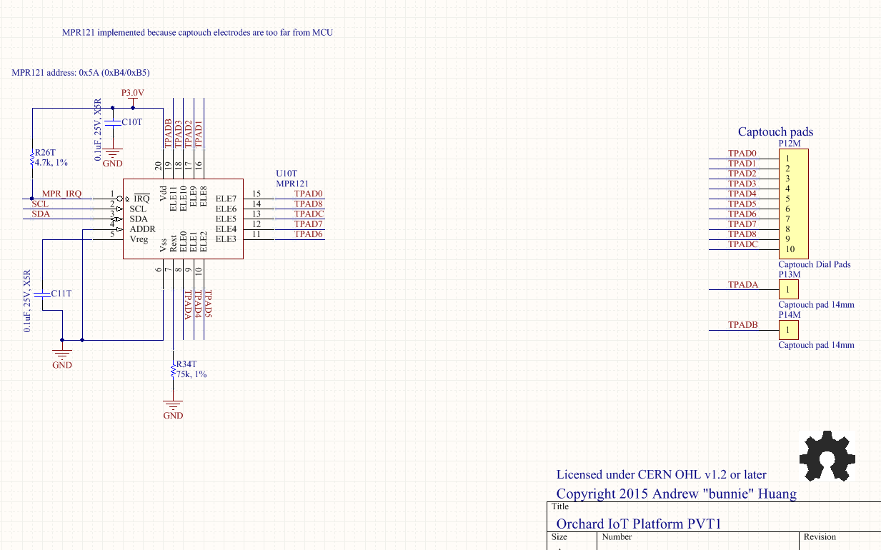
While the Kinetis MCU supports captouch on its own, we opted not to use the facility because it's poorly documented, and the scant documentation we could find indicated that the traces should be shorter than about 4-5". The problem is that we wanted to co-locate the MCU next to the RF port, which isn't always convenient for captouch surfaces. Thus to improve our chances of first-time success, we opted to use an external captouch chip with better documentation and board location.
We steered clear of using any of the DIO pins for any GPIO purposes. We opted to connect the RF packet ready and transmission FIFO not full (TX_CAN) pins, so that we could use interrupts to drive automatic FIFO filling and draining for reliable implementation of larger packet lengths without busy-waiting the CPU in a thread monitoring FIFO status.
As an administrative note, we use the schematic symbols "NT" to indicate components that are part of the BOM but not assembled onto the board. So, for example, the firmware and the antenna (which screws into the SMA edge launch socket) are NT symbols.
GPIO Expander Although we could just barely cram all the signals into the MCU for the base design, as a platform we needed to have some free pins for extensibility. Thus, we included a GPIO expander. For cost-down designs that don't need to support such a rich set of peripherals, one could certainly cut the GPIO expander from the design and rework the firmware to use direct GPIO mappings.
Our choice of which pins to route to the GPIO expander was primarily static signals (reset lines, charger status lines) and less time sensitive interrupts. The GPIO expander can aggregate interrupts and fire a single pin that's then handled by firmware that queries the exact interrupt source and dispatches the correct routine based on that query.
LDO The LP3982 LDO is a reasonably inexpensive LDO (~$0.20) with very low dropout, good noise performance, and 90uA quiescent current. Cheaper LDOs can be substituted, but compared to the cost of other components in the system it seemed like a reasonable compromise between cost and performance.
The quiescent current is a bit high compared to the ultimate performance achievable by the Kinetis-W (
The 300mA output of the LDO is ample for the system.
Charger & Battery
Sensors
OLED
BLE
LED
Captouch
High-Res Photo Guide
